▶️ Watch on YouTube …
This post is about the evaluation of the DC-DC Boost Converter in Synchronous and Non-Synchronous by utilizing the same hardware with different coding. In my previous post about DC-DC Boost Converter using Arduino Uno, it only discussed non-synchronous..
Introduction
A DC-DC converter is an electronic device used to convert DC voltage from one voltage level to another. Here we will discuss the two types of DC-DC converters that are often used, namely synchronous and non-synchronous. Both have different characteristics and uses. Let’s take a closer look.
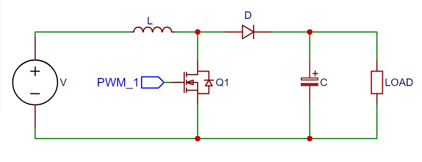
DC-DC Boost Converter Non-Synchronous
A non-synchronous boost converter, also known as an asynchronous step-up converter, is a type of DC-DC converter that uses a diode as the primary element to allow current to flow when the transistor is in the non-conducting state.
Following are some of the characteristics and advantages of a non-synchronous boost converter:
Advantages:
Simple and Inexpensive:
The non-synchronous boost converter has a simpler design and lower manufacturing costs compared to the synchronous variant.
Suitable for Light Loads:
This converter is suitable for applications that have light loads and do not require high control precision.
Disadvantages:
Low Efficiency:
Non-synchronous boost converters tend to have lower efficiencies due to significant diode losses when operating in the non-conducting state.
Quality of Control Decreases:
Current and voltage controls are not as precise as synchronous converters, especially in applications where high precision is required.
Not Suitable for Heavy Loads:
This converter is not suitable for heavy loads or applications where a more stable and accurate voltage level is required.
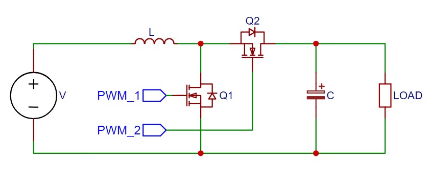
DC-DC Boost Converter Synchronous
A synchronous boost converter, also known as a synchronous step-up converter. Is a type of DC-DC converter in which the synchronization between a power switch duty cycle and a synchronous current change is accomplished through the use of a synchronous transistor (MOSFET) together with a diode. The diode is used in these converters as a current path when the synchronous transistor is in the non-conducting state (just before the conduction transistor).
Following are some of the characteristics and advantages of a synchronous boost converter:
Advantages:
Higher Efficiency:
Tend to have higher efficiencies due to the minimal diode losses that occur in the non-conducting transistor state.
Better Control:
With synchronous transistors, control over current and voltage flow can be improved. The result is better performance in applications where control precision is required.
Disadvantages:
Higher Cost:
Synchronous boost converters are usually more expensive as they require additional synchronous transistor components and more complex monitoring.
Design Complexity:
The design and implementation of a synchronous boost converter can be more complicated than the non-synchronous version.
Synchronous or Non-synchronous configuration via Coding
By adjusting the output signals for MOSFETs Q1 and Q2 through coding, I can test both configurations of the DC-DC Boost Converter.
The PWM_1 signal on Q1 is the signal that will control the converter’s output voltage by adjusting the PWM pulse width. This pulse width adjustment on Q1 is used in both synchronous and non-synchronous configurations. When Q1 is On, the inductor L is connected to the negative rail, and at that time, the inductor is charged. Then, when Q1 turns Off, the voltage from the inductor which is greater than the input voltage will be output through the diode or switch Q2.
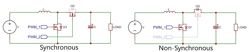
MOSFET Q2 is the one I configured to operate as either non-synchronous or synchronous.
For the non-synchronous configuration, you leave Q2 without control pulses, meaning Q2 always stays in the Off state. Because Q2 is Off, the voltage from the inductor L, which is higher than the voltage across capacitor C, is passed to capacitor C through the body diode of Q2.
When I want to configure it as synchronous, I need the PWM_2 signal on Q2, which is the complement of PWM_1. This means that when PWM_1 is On, PWM_2 is Off, and vice versa. When the PWM_2 signal is On, the voltage across inductor L will be passed to capacitor C through the switch, not through the body diode of MOSFET Q2.
DC-DC Boost Converter Design
Here is a step-by-step guide that I did to design a DC-DC Boost Converter:
Design Specification
Before starting the design, I define the design specifications which include parameters such as input voltage, output voltage, output current, desired efficiency, and operating frequency, as follows:
| Parameter | Value |
| PWM frequency | 31.25 kHz |
| Input Voltage | 9 Volt – 12.0 Volt |
| Output Voltage | 13 Volt – 30 Volt |
| Output Current | 5 Amps |
Component Selection
As in my previous project about DC boost converter, here I also use the same method to determine the components used. Namely by using the DC-DC boost converter calculator from Adafruit.
Using the DC-DC boost converter calculator from Adafruit the results are as follows:
| Minimum Duty Cycle | 7.69 % |
| Maximum Duty Cycle | 70 % |
| Minimum Inductor Size | 9.216 uH |
| Peak Inductor Current | 25 A |
| Minimum Capacitor | 1600 uF |
| Minimum Schottky Diode | 30 V / 25 A |
The value of the Duty Cycle parameter is the value that will be used for PWM generation in coding.
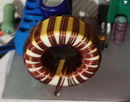
I made the necessary inductor using a T90-26 yellow-and-white toroid core. I wrapped the core in 20 turns using three 0.5mm wires (AWG24). Measurements using the LCR meter show a value of 20 uH exceeding the minimum required value. I assume the ability of the inductor to pass current at the Peak Inductor Current is sufficient. Many things must be considered to design a power inductor properly, so for the time being I work based on the assumptions first.
Next about the required capacitor. The result of the calculation is that a minimum of 1600 uF is required. The capacitor voltage I choose must be greater than the maximum output voltage, the capacitor value of 1600uF/50V I think is sufficient.
Finally regarding Diodes and MOSFETs. The stock MOSFET that I currently have is IRF3205 and after I match it with the datasheet I conclude that I can use IRF3205 in this project. Evaluation is mainly on current and voltage parameters both on the MOSFET and on the Body Diode.
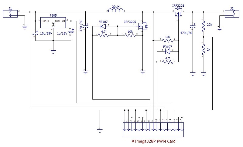
Circuit Design
I made the DC-DC Boost Converter circuit into two parts, namely the power part and the PWM controller part.
Power section Circuit
The circuit I made is in accordance with the basic circuit of the boost converter using the component values above. The circuit is as follows:
Many things must be considered in making a PCB layout, such as connection lines, ground plane areas, and others to minimize interference and power loss. Before knowing a good way to design a PCB for this purpose, I tried to make a PCB layout based on circuit connections only.
PWM Circuit
In order not to make a PCB for PWM signal generation, I use an ATmega328P PWM Card. Please see my post about this for more details. Not all parts of the circuit were used in this project, the circuit with a blue background is the part I used in this experiment.
Code
In this project, I will implement a DC-DC Boost Converter using the ATmega328 microcontroller. The code aims to control the operation of the Boost Converter through Pulse Width Modulation (PWM) and regulate the output voltage based on the comparison of the feedback voltage with the reference voltage.
Variable Declaration
The code begins by declaring the microcontroller pins that will control the semiconductor switch. Additionally, it sets the desired crystal frequency and PWM frequency. These parameters serve as the basis for calculating the PWM duty cycle and dead time.
const byte vfbPin = A0;
const byte potPin = A3;
const byte pwmOutA = 9;               // PB1 OC1A
const byte pwmOutB = 10;              // PB2 OC1B

const long fXTAL = 16000000;          // crystal freq.
const int fPWM = 31250;               // fMax 31250 Hz
const int icr = ((fXTAL / fPWM) / 2);
const int deadTime = 5;               // deadTime = 62.5nS * 5 = 312.5nS

volatile int dutyOn = icr * 0.1;
int analogReadTolerance = 4;          // adjust as needed (compensation for noise and component tolerances)
int voltageReff = 307;                // preset output @ 18V  (1.5V @ vfbPin)
Port Initialization
The initPort() function is used to initialize the microcontroller pins used to control the semiconductor switch.
void initPort() {
  pinMode(pwmOutA, OUTPUT);
  pinMode(pwmOutB, OUTPUT);
}
Timer Initialization
The initTimer() function is used to configure the microcontroller’s timer, including synchronous and asynchronous modes. In this code, the non-PWM mode is selected to control the Boost Converter’s operating conditions. Additionally, the PWM frequency and the top value of the counter (ICR1) are set as previously declared.
void initTimer() {
//  TCCR1A = 0b00110000;    // non-Sync Boost converter configuration (OC1A disable OC1B enable)
  TCCR1A = 0b10110000;     // Sync Boost ( OC1A & OC1B enable)
  TCCR1B = 0b00010001;    //WGM1 3:2 = 10 (Waveform Generation Mode 8), CS1 2:0 = 001 (no prescale)
  TIMSK1 = 0b00000001;    // xxxxxxx1 TOV1, interrupt when counter overfow.
  ICR1 = icr;             // Counter TOP value.
  OCR1B = icr - dutyOn;               // init lowside switch (sync & non sync operation)
  OCR1A = icr - dutyOn - deadTime;    // init highside switch (sync only)
}
The code above is for testing the DC-DC boost synchronous operation. For non-synchronous operation, uncomment the code in the first line and comment out the code in the second line.
I’ve chosen waveform generation mode 8, which is Phase and Frequency Correct mode. In this mode, the counter operates as an Up-Down Counter, resulting in a virtual triangular waveform. If I were to use a fast PWM mode, for example, the generated signal would be a sawtooth waveform.
I’m using mode 8 to be able to insert dead time at the beginning and end of the generated PWM pulses. If I were to use fast PWM mode, I could only insert dead time at the beginning or end of the pulse.
In a DC-DC Boost Converter Synchronous system, two switches work alternately, so dead time is necessary to ensure that they do not activate simultaneously. During the dead time, the body diode works briefly before the switch (MOSFET) operates.
In a Non-Synchronous system, since only one switch is used, Dead-time parameters are not required. Basically, when Q1 is off, it represents dead time (all MOSFETs are off).
Interrupt Service Routine (ISR)
The ISR (Interrupt Service Routine) function works when an overflow occurs on the microcontroller’s timer. In this section, the duty cycle value is recalculated, and the values of OCR1A and OCR1B are set to control the semiconductor switch.
ISR(TIMER1_OVF_vect) {
  int temp = icr - dutyOn;
  OCR1A = temp - deadTime;
  OCR1B = temp;
}
Setup
The setup section initializes the ports and timer using the functions that were defined previously. This is where you configure the microcontroller’s hardware settings to prepare it for the specific operation of the DC-DC Boost Converter.
void setup() {
  initPort();
  initTimer();
}
Loop
The main loop of this code is responsible for controlling the operation of the Boost Converter based on the comparison between the feedback voltage and the reference voltage. If the feedback voltage exceeds a certain upper limit, the duty cycle is reduced, and if the feedback voltage is lower than a certain lower limit, the duty cycle is increased. This feedback control loop helps regulate the output voltage of the Boost Converter to maintain it within the desired range.
void loop() {

  int voltageFeedBack = analogRead(vfbPin);
  if (voltageFeedBack > (voltageReff + analogReadTolerance)) {
    dutyOn--;
  } else if (voltageFeedBack < (voltageReff - analogReadTolerance)) {
    dutyOn++;
  }
}
Feedback for this DC-DC Boost Converter is obtained by reading the output voltage, which is first attenuated through a voltage divider. The voltage on the input port (vfbPin) is continuously read and compared to the reference voltage. The reference voltage value represents the desired output voltage. When there is a difference between the feedback and reference values, the output is corrected by adjusting the duty cycle.
This code regulates the output voltage based on the voltage feedback, with the goal of effectively controlling the output power. However, it’s important to note that this code outlines the basics of Boost Converter implementation and further adjustments may be needed for optimal performance.
Setting-Up and Testing
The hardware setup for the testing I will conduct is as shown in the following diagram:
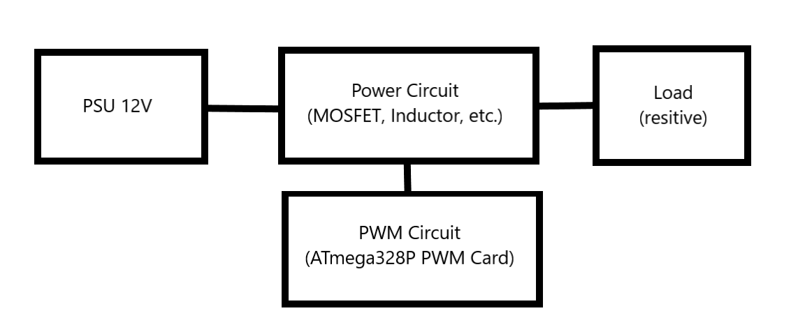
In testing both the synchronous and non-synchronous DC-DC Boost Converter, there are no hardware changes whatsoever. The difference lies solely in the code uploaded to the ATmega328P.
Preliminary Test
The first test of the DC-DC Boost Converter Synchronous without a load yielded a voltage output of 18.0 V with an input voltage of 12 V.
When I added a load of 1.5 Amps, the voltage remained at 18.0 V, but there was an anomaly: the ATmega328P PWM card frequently experienced unexpected resets.
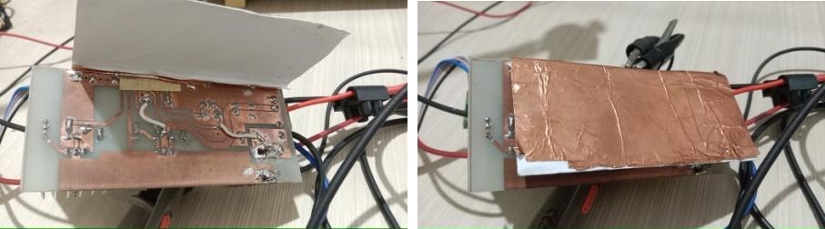
The likely cause of this issue is a poor PCB layout, which is generating significant RFI/EMI interference. To attempt to address this, I applied copper tape beneath the PCB as a ground plane.
I have successfully resolved the reset issue, so the next testing phase will proceed under these conditions.
Note: I don’t share the PCB layout due to the bad layout design.
DC-DC Boost Converter Synchronous Test
I conducted the Synchronous mode test by configuring TCCR1 as follows:
void initTimer() {
// TCCR1A = 0b00110000; // non-Sync Boost converter configuration (OC1A disable OC1B enable)
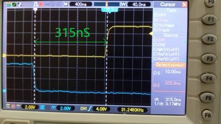
TCCR1A = 0b10110000; // Sync Boost ( OC1A & OC1B enable)The dead-time I obtained is approximately 315 nS, which is quite close to the expected value of 312.5 nS. The picture below illustrates the dead time, which is the period during which both signals are logic LOW.
Here are the control signals for both MOSFETs (Yellow for Q1 and blue for Q2):
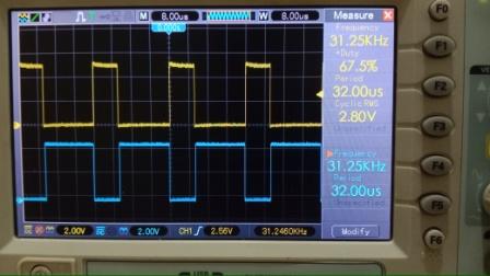
The measurement results for Vin 12V and Vout 18V are as follows:
| Parameter | No Load | With Load @5A |
| Input Current (A) | 0.210 | 8.27 |
| Duty Cycle (%) | 32 | 37.1 |
In this configuration, I observed that there is no significant increase in temperature for both MOSFETs.
DC-DC Boost Converter non-Synchronous Test
I conducted the non-synchronous mode test by configuring TCCR1 as follows:
void initTimer() {
  TCCR1A = 0b00110000;    // non-Sync Boost converter configuration (OC1A disable OC1B enable)
//  TCCR1A = 0b10110000;     // Sync Boost ( OC1A & OC1B enable)
In this test, I didn’t perform a Dead-Time measurement because, in this configuration, only one MOSFET is operating.
The control signal is as follows (Yellow for Q1 and blue for Q2):
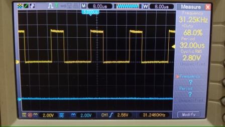
The measurements are as follows:
| Parameter | No Load | With Load @5A |
| Arus Input (A) @12V | 0.099 | 8.72 |
| Duty Cycle | 12.5 | 39.9 |
In this configuration, there is a noticeable increase in temperature for the diode (MOSFET Q2).
Evaluation
PCB
In my initial testing, I encountered the issue of the microcontroller resetting itself, and the preliminary suspicion is that there was interference due to switching. By adding copper tape to enhance the ground plane, this interference issue was effectively resolved. In the PCB design, there are several traces carrying significant power, and these traces should be carefully designed to minimize interference.
Inductor
The temperature increase in the inductor, even during no-load operation, in both synchronous and non-synchronous configurations, could indeed indicate that the inductor you have used may not be suitable for this application. It’s important to select an inductor with the appropriate specifications, including its current rating and core material, to ensure efficient and safe operation in your DC-DC Boost Converter circuit. The inductor plays a crucial role in energy storage and transfer in these circuits, and using an inadequate one can lead to increased losses and temperature rise. Consider reviewing the inductor specifications and possibly selecting a different one to better suit your needs.
MOSFET Temperature
In the Synchronous configuration, it’s observed that the temperature of MOSFETs Q1 and Q2 remains relatively stable even when the DC-DC Boost Converter is loaded.
However, in the Non-Synchronous configuration, MOSFET Q2 experiences a noticeable increase in temperature, especially when a load is applied. This occurs due to a voltage drop across the diode, as the forward voltage across the diode results in power dissipation in the form of heat.
It’s important to consider these temperature variations and their causes in your design, as they can impact the efficiency and reliability of the DC-DC Boost Converter. Proper heat sinking or component selection may be necessary to manage temperature increases in critical components like MOSFETs and diodes.
Efficiency
From the measurements above, at an output power of 90 Watts (5 Amps x 18 Volts), I obtained the following efficiency values:
Eff = (Pout / Pin) x 100%
In the Synchronous configuration:
Input Power: Pin = 8.27 Amps x 12 Volts = 99.2 Watts
Efficiency = (90 / 99.2) x 100% = 91%
In the Non-Synchronous configuration:
Input Power: Pin = 8.72 Amps x 12 Volts = 104.6 Watts
Efficiency = (90 / 104.6) x 100% = 86%
These efficiency values indicate the percentage of input power that is successfully converted to output power for each configuration. The Synchronous configuration appears to be more efficient compared to the Non-Synchronous configuration for the given load and input voltage conditions.
Conclusion
In this project, I explored the two common types of DC-DC Boost Converters: Synchronous and Non-Synchronous. Each type has its own advantages and disadvantages.
The Non-Synchronous DC-DC Boost Converter is simple and cost-effective, making it suitable for applications with light loads that do not require high control precision. However, it tends to have lower efficiency due to significant diode losses in the non-conducting state and may not be suitable for heavy loads or applications requiring precise voltage control.
On the other hand, the Synchronous DC-DC Boost Converter offers higher efficiency, better control over current and voltage, and the ability to recover energy stored in the inductor’s magnetic field. However, it comes at a higher cost and involves more complex design and monitoring.
Both configurations were tested using an ATmega328P microcontroller, with careful consideration of hardware design, component selection, and code implementation. Notable observations included the need for a proper PCB layout to minimize interference, the importance of selecting an appropriate inductor, and the temperature variations in critical components like MOSFETs and diodes.
Efficiency measurements showed that the Synchronous configuration outperformed the Non-Synchronous configuration in terms of power conversion efficiency.
Overall, the choice between Synchronous and Non-Synchronous DC-DC Boost Converters depends on the specific requirements of the application, including load conditions, control precision, and cost considerations. Designers should carefully evaluate these factors to select the most suitable configuration for their needs.
Code Listing
/*
   ATmega328_PWM_Boost_sync.ino

   Created : 20 June 2023
   Author  : yopie DIY

   PWM clock = fXTAL/freqPWM = 16,000,000/10,000 = 1,600 clock.
   WGM mode 8 is used, so ICR1 = 1,600/2 = 800 clk
*/

const byte vfbPin = A0;
const byte potPin = A3;
const byte pwmOutA = 9;               // PB1 OC1A
const byte pwmOutB = 10;              // PB2 OC1B

const long fXTAL = 16000000;          // crystal freq.
const int fPWM = 31250;               // fMax 31250 Hz
const int icr = ((fXTAL / fPWM) / 2);
const int deadTime = 5;               // deadTime = 62.5nS * 5 = 312.5nS

volatile int dutyOn = icr * 0.1;
int analogReadTolerance = 4;          // adjust as needed (compensation for noise and component tolerances)
int voltageReff = 307;                // preset output @ 18V  (1.5V @ vfbPin)

void initPort() {
  pinMode(pwmOutA, OUTPUT);
  pinMode(pwmOutB, OUTPUT);
}

void initTimer() {
//  TCCR1A = 0b00110000;    // non-Sync Boost converter configuration (OC1A disable OC1B enable)
  TCCR1A = 0b10110000;     // Sync Boost ( OC1A & OC1B enable)
  TCCR1B = 0b00010001;    //WGM1 3:2 = 10 (Waveform Generation Mode 8), CS1 2:0 = 001 (no prescale)
  TIMSK1 = 0b00000001;    // xxxxxxx1 TOV1, interrupt when counter overfow.
  ICR1 = icr;             // Counter TOP value.
  OCR1B = icr - dutyOn;               // lowside switch (sync & non sync operation)
  OCR1A = icr - dutyOn - deadTime;    // highside switch (sync only)
}

void setup() {
  initPort();
  initTimer();
}

void loop() {
  int voltageFeedBack = analogRead(vfbPin);
  if (voltageFeedBack > (voltageReff + analogReadTolerance)) {
    dutyOn--;
  } else if (voltageFeedBack < (voltageReff - analogReadTolerance)) {
    dutyOn++;
  }
}

ISR(TIMER1_OVF_vect) {
  int temp = icr - dutyOn;
  OCR1A = temp - deadTime;
  OCR1B = temp;
}